www.industry-asia-pacific.com
27
'15
Written on Modified on
THROUGH THICK AND THIN – A GUIDE TO THICK AND THIN FILM COATING OF CERAMICS
Oliver Ridd of Morgan Advanced Materials discusses coating technologies, their applications and performance benefits

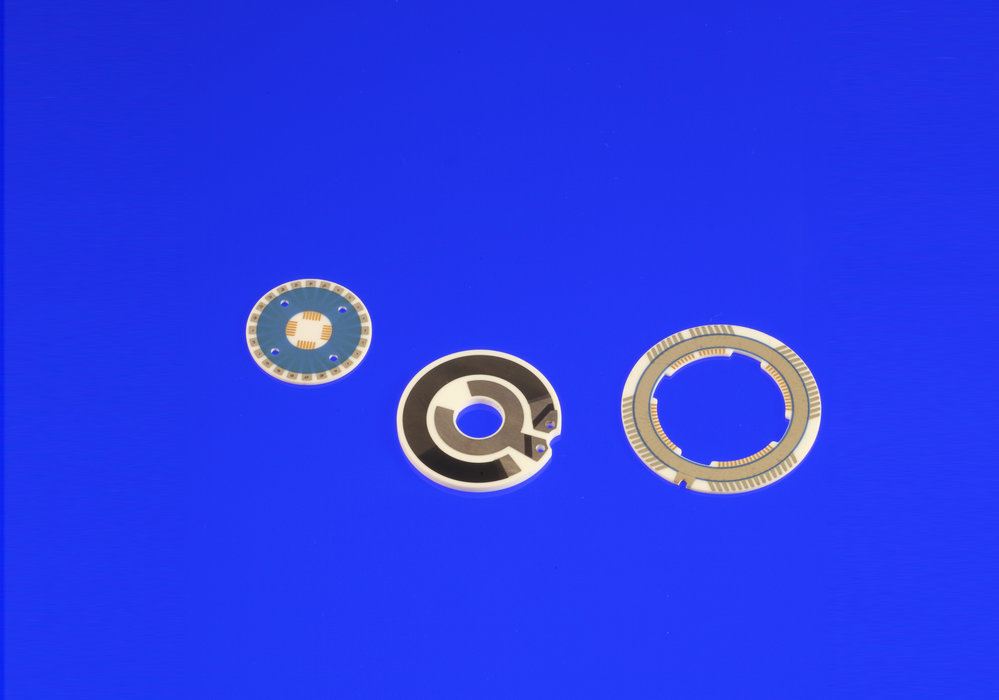
Providing a range of functions including solderable conductors, dielectric components and resistors, the thick film process provides a bonded coating on the surface of alumina ceramics. The process involves the application of a specialist coating via techniques, which vary depending on the geometry of the product. The most common of these are screen printing and brush coating. For intricate designs, on flat surfaces, screen printing is the most suitable method – the process itself is the only limiter on complexity - whereas brush coating is ideal when working with radial surfaces. Thick film coating materials vary according to each application but can include silver, silver palladium, silver platinum, copper and gold, as well as a variety of resistor inks. Normally with a thickness in the region of 10-12 microns, coatings are fired onto the ceramic at around 850°C to ensure a strong bond. Where conventional materials can fail as temperatures reach in excess of 150°C, thick film technology remains stable at high temperatures.
Another key application is the printing of circuit board technology onto ceramics – creating printed circuits which are strong enough to accept soldered joints and/or wire bonded connections. This type of application is common in sectors including aerospace, microelectronics, security and healthcare, offering greater scope for more complex patterns often built up in multiple layers to create dense hybrid networks that take minimal area. Ceramic substrates can even be glaze-bonded together, providing hermetic joints with or without printed circuitry in between. They are able to function in a wide range of environments, where their properties make them more resistant to excessive heat, moisture, corrosion and shock.
Morgan Advanced Materials has the capability to manufacture parts with intricate geometries and shapes, customised for individual requirements. The manufacture of the underlying alumina ceramic is done in-house using Morgan’s proven materials which further increases the customer’s options for a tailored end product. While Deranox™ 975 alumina is utilised for many applications, other alumina grades are available and can be matched to customer’s specific requirements. Thick film technology can be used in a variety of applications such as instrumentation, control and guidance systems, as well as IR and UV detectors. Other materials available include clear glazes and coloured dielectrics, while the facility for electroplating offers further additional options. The versatility of Morgan’s thick film coated products coupled with the company’s Application Engineers’ design expertise enables their use in situations where a suitable product might not previously have been available.
Thick film coating is a relatively inexpensive process, with low tooling costs. Furthermore, with lead times ranging between four and six weeks depending on the complexity of the product, turnaround is quicker than many alternative technologies currently available.
If thick film coating is not an option, Morgan can also offer thin film coating technology. Thin film coatings usually measure somewhere between one and two microns and are typically selected where circuit complexities demand fine track widths and spaces or geometries are small and complex. As well as gold and silver, other materials such as titanium, nickel, aluminium and chrome are also suitable for use as a coating and can be applied to piezo ceramics. In this instance, it is applied using Physical Vapour Deposition, otherwise known as sputter coating. Although more expensive, it is a necessity in certain applications, where a higher level of purity is required for products to function correctly and to avoid the risk of contamination – such as in the healthcare sector. Thin film coating ensures excellent replication of ceramic surface finish and also allows for the possibility of profiled patterns. Similarly, it is possible to apply multiple layers and electroplating.
Thick and thin film coatings offer customers the ability to incorporate a range of functions and performance attributes within their devices, without excessive cost and in most applications, with greater precision than alternative methods. As more and more sectors become aware of these technologies, we can expect to see a wider uptake of both of them as the drive continues to develop compact, multi-function components able to withstand demanding environments, without compromising performance.
For further information visit: http://www.morgantechnicalceramics.com/products/product-groups/metallised-ceramic-components

