
www.industry-asia-pacific.com
25
'26
Written on Modified on
Nidec to Showcase PCB Inspection Solutions at THECA 2026
Nidec will present its electrical, optical, and X-ray inspection equipment for printed circuit boards and semiconductor substrates at THAILAND ELECTRONICS CIRCUIT ASIA (THECA) 2026.
www.nidec.com
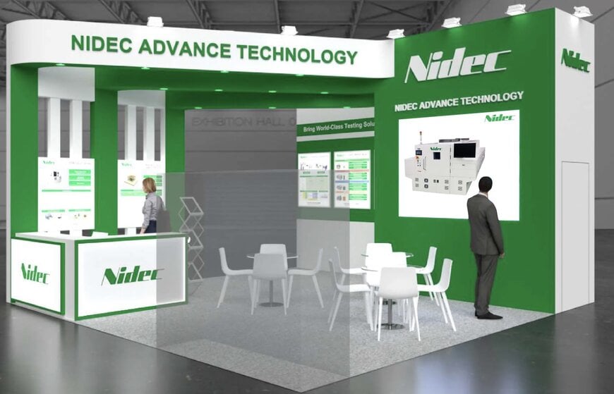
Nidec Advance Technology Corporation announced it will exhibit at THECA 2026, held at the Bangkok International Trade & Exhibition Centre (BITEC) from August 26 to August 28, 2026, at Booth R13. Hosted by the Thailand Printed Circuit Association, the trade event focuses on printed circuit boards (PCBs) and printed circuit board assemblies (PCBAs).
Quality Control and Electrical Testing Systems
The showcase focuses on quality assurance across high-density, multi-layer circuit boards and advanced packaging. Nidec Advance Technology’s electrical testing systems detect internal structural defects, conduction continuity, and isolation leakage across high-density interconnect (HDI) substrates and semiconductor packages:
- STAR REC Series: Electrical continuity and short-circuit testing equipment engineered for HDI and multilayer PCB substrates.
- GATS Series: Conduction and isolation testing systems designed for high-density semiconductor package substrates.
- GATS-8360: Large-format electrical inspection platform for oversized multi-up substrate panels.
- Custom High-Precision Jigs: Dedicated test fixtures and probe arrangements designed to maintain stable electrical contact and prevent false-call rejection rates.
Optical, AI, and X-Ray Metrology Portfolio
The company will also demonstrate automated optical, 3D metrology, and radiographic testing systems:
The company will also demonstrate automated optical, 3D metrology, and radiographic testing systems:
- High-Speed CT X-Ray Inspection: Debuting for the first time in Thailand, this computed tomography system delivers volumetric non-destructive evaluation of internal substrate structures and back-drilled via depths.
- AURCA Series: AI-driven 3D automated final visual inspection (AFVI) system designed for optical modules and large-format substrates.
- RWi-300MK3: 2D and 3D automated optical inspection system engineered for wafer-level micro-bump height and coplanarity verification.
- RSH Series: High-resolution 2D and 3D optical inspection equipment for fine-pitch high-density substrates.
Additional Context
This section details technical specifications not included in the original news release.
Back-drilling, or controlled-depth counter-boring, removes unused conductive via stubs in multi-layer high-speed digital circuit boards to eliminate signal reflections, jitter, and deterministic insertion loss at transmission rates exceeding 56 and 112 gigabits per second per channel. High-speed computed tomography X-ray systems utilize micro-focus X-ray tubes and digital flat panel detectors to reconstruct 3D volumetric slices, measuring the remaining stub length with single-digit micrometer precision to verify that conductive stubs do not exceed strict design tolerances without severing active inner-layer trace connections.
In electrical testing of advanced flip-chip ball grid array (FC-BGA) packages and substrate-like PCBs (SLP), high-density bare-board testers employ four-wire Kelvin resistance measurement methods and micro-electro-mechanical systems (MEMS) spring probe pins. These probe arrays achieve contact pitches under 50 micrometers while applying controlled contact forces (often between 1 and 3 grams-force per pin) to prevent pad deformation. Optical 3D wafer bump inspection platforms leverage structured white-light interferometry or multi-angle laser triangulation to measure micro-bump coplanarity, diameter, and position across 300 mm wafers at inspection throughputs exceeding several thousand bumps per second.
Edited by Romila DSilva, Induportals Editor, with AI assistance.
This section details technical specifications not included in the original news release.
Back-drilling, or controlled-depth counter-boring, removes unused conductive via stubs in multi-layer high-speed digital circuit boards to eliminate signal reflections, jitter, and deterministic insertion loss at transmission rates exceeding 56 and 112 gigabits per second per channel. High-speed computed tomography X-ray systems utilize micro-focus X-ray tubes and digital flat panel detectors to reconstruct 3D volumetric slices, measuring the remaining stub length with single-digit micrometer precision to verify that conductive stubs do not exceed strict design tolerances without severing active inner-layer trace connections.
In electrical testing of advanced flip-chip ball grid array (FC-BGA) packages and substrate-like PCBs (SLP), high-density bare-board testers employ four-wire Kelvin resistance measurement methods and micro-electro-mechanical systems (MEMS) spring probe pins. These probe arrays achieve contact pitches under 50 micrometers while applying controlled contact forces (often between 1 and 3 grams-force per pin) to prevent pad deformation. Optical 3D wafer bump inspection platforms leverage structured white-light interferometry or multi-angle laser triangulation to measure micro-bump coplanarity, diameter, and position across 300 mm wafers at inspection throughputs exceeding several thousand bumps per second.
Edited by Romila DSilva, Induportals Editor, with AI assistance.
