
www.industry-asia-pacific.com
20
'17
Written on Modified on
MID in pole position
Three-dimensional molded interconnect devices
Three-dimensional molded interconnect devices are a welcome addition to conventional printed circuit boards and are particularly well suited to Industry 4.0 applications. The example of a smoke detector illustrates how design and functional integration are simplified with this technology.
Whether rigid or flexible, printed circuit boards are a virtually indispensable part of electronic devices as interconnect devices. Plastic molded interconnect devices (MIDs) offer many advantages with regard to connection technology, including the combination of electrical and mechanical functions in a single component. This makes it possible to use the housing and other molded inner structures as an interconnect device, sometimes eliminating the need for a PCB.
Three-dimensional functional integration
The MID is a multifunctional component with sensors arranged and aligned with a high precision combined with an RFID antenna for sending and receiving signals. This concentration of functions on a single carrier material enables development engineers to create three-dimensional microelectromechanical systems (MEMS). MIDs are ideally suited for this purpose, particularly when manufacturing large and very large volumes.
MID technology in detail
Three-dimensional MIDs are manufactured using the LDS (laser direct structuring) method: The shape of the interconnect device desired by the customer is created in a single-component injection molding process, which offers virtually unlimited freedom for three-dimensional design.
While conventional printed circuit boards use FR4 fiberglass fabric or similar base material, molded interconnect devices are built from thermoplastics. The thermoplastic base material is first compounded with a (nonconductive) laser-activated metal-organic additive.
The LDS laser beam structures the circuit pattern onto the device by cleaving the metal-organic additives while roughening and ablating the plastic precisely where the beam strikes the surface. Copper seeds split out from the additive, attracting free copper in the subsequent metallization step.
In the following electroless metallization process within a copper bath the copper seeds created in the lasering step now attract solid copper out of solution. After copper plating, electroless nickel and immersion gold (ENIG) layers may be added to the copper layer. When an MID is not soldered or bonded, nickel alone over copper is sufficient. ENIG metallization ensures good surface properties for designs where SMT soldering or Wire-Bonded component placement is desired.
Potential of the technology
In modern connection technology, engineers use flex or rigid-flex printed circuit boards or wires if an electrical connection is to be established between several printed circuit boards in various positions and alignments. Here the core benefits of the MIDs allows a reduced number of parts, resulting in process, material, and logistics savings while at the same time raising quality with the reduction of assembly steps and expenses. MID technology holds enormous potential for functionally oriented product development with optimized manufacturing processes.
Flexible printed circuit boards are often a suitable solution for bypassing physical distances at changing angles but for the precise positioning and fixing of sensors such as Hall-effect sensors or LED lighting on Flex, this incurs extra costs. The MID component enables possibilities in the microscale and is unbeatable here, with the precise positioning of components and defined angles in arrangements being easy to realize. To achieve a fully realized MID product, antennas or shields can be attached to the carrier and connected to the circuit. Circuit density has been achieved in large series production with an 80µm circuit trace / 80µm space and contributes to greater opportunity for miniaturization.
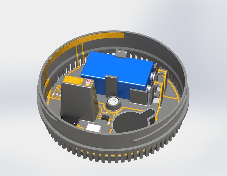
Example: smoke detectors
Today's smoke detectors are ideally suited for upgrading to MID technology. The carrier material for smoke detectors today is made up of plastic components and provides a molded part to which the components may be fixed.
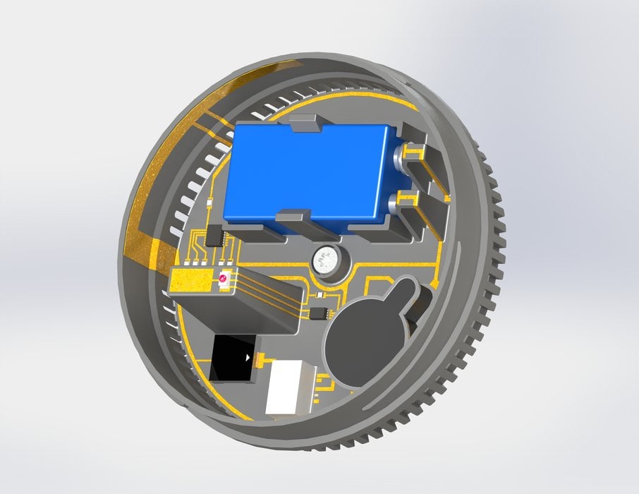
MID technology enables significant simplification of the design and the functional integration associated with the smoke detector. The battery holder is integrated directly in the MID part, thus forming all the metal contacts. The two connecting cables and the elaborate soldering process for bonding are now redundant. Standard SMDs can be soldered directly to the plastic, thereby saving costs while also allowing placement to be performed using pick-and-place machines, reducing personnel expenses for the assembly process to a minimum. The number of components is also reduced to a minimum – the printed circuit board is no longer required and circuit paths inscribed directly on the plastic replace the wires, which means that connecting plugs are also not needed.
Moreover, it is easy to integrate antennas in order to network the smoke detectors. By adapting the laser programming, any antenna structure can be applied directly to the same carrier material. Last but not least, because the MID technology eliminates the need for mechanical switches, it is simple to metallize a capacitive surface and use it as a capacitive switch.
Proven in industry
Three-dimensional MID technology has long been tried and tested in industry. It was first employed for the challenges of spatial antenna construction, as well as for expanding frequency ranges, integration densities and available installation spaces for high-frequency applications. Molded interconnect devices are suitable for 3D antennas in frequency ranges exceeding 6 GHz, reliable for Bluetooth, LTE or Wi-Fi applications. Antennas manufactured using this procedure can be found in billions of smartphones, tablets and other portable devices.
Millions of mobile payment terminals also contain MID solutions. All known areas of industry in which currents flow or shielding is necessary harbor countless possible applications for molded interconnect devices. Furthermore, the mechatronic advantages of the technology enable holders to be designed for energy sources such as button batteries, making the interconnect device an elegant solution.
Multiple Dimensions AG
Multiple Dimensions is world's leading technology enterprise specializing in the development of customized molded interconnect devices and their production. Multiple Dimensions AG maintains close partnerships with its customers across the entire process chain, from device design through large-scale series parts production. Multiple Dimensions AG is worldwide represented.
