APPLIED MATERIALS INTRODUCES NEW PLAYBOOK FOR PROCESS CONTROL BASED ON BIG DATA AND AI
Applied Materials, Inc. today unveiled a major innovation in process control that uses Big Data and AI technology to help semiconductor manufacturers accelerate node development, speed time to revenue and earn more profits over the life of a node.

- New Enlight® optical wafer inspection system combines breakthrough performance with new optics that capture more yield data from every wafer
- ExtractAI technology uses the power of AI to quickly classify yield-killing defects and remove noise
- Fastest-ramping inspection system in Applied Materials history helps customers accelerate node development, ramp to high volume faster and sustain higher yields
Semiconductor technology is becoming increasingly complex and expensive, and reducing the time needed to develop and ramp advanced nodes can be worth billions of dollars to chipmakers around the world. Success is gated by the ability to detect and correct defects which is becoming increasingly difficult as line widths shrink and turn nuisance particles into yield killers. Likewise, 3D transistor formation and multiprocessing techniques introduce subtle variations that can multiply to create yield-killing defects that are vexing and time-consuming to root-cause.
Applied Materials is solving these challenges with a new playbook for process control designed to bring the benefits of Big Data and AI technology to the core of chipmaking technology. Applied’s solution consists of three elements that work together in real time to find and classify defects faster, better and more cost effectively than legacy approaches. The three elements are:
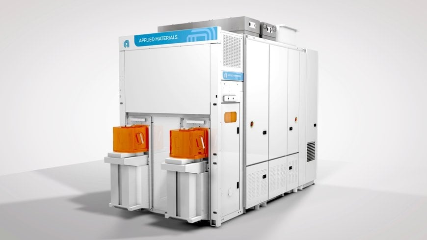
New Enlight® Optical Wafer Inspection System: in development for five years, the Enlight system combines industry-leading speed with high resolution and advanced optics to collect more yield-critical data per scan. The Enlight system architecture improves the economics of optical inspection, resulting in a 3x reduction in the cost of capturing critical defects as compared to competing approaches. By dramatically improving cost, the Enlight system allows chipmakers to insert many more inspection points in the process flow. The resulting availability of Big Data enhances “line monitoring,” statistical process control methods that can predict yield excursions before they occur, immediately detect excursions so that wafer processing can be halted to protect yields, and enable root-cause traceback to accelerate corrective actions and the return to high-volume manufacturing.
New ExtractAI Technology: developed by Applied’s data scientists, ExtractAI technology solves the most difficult problem of wafer inspection: the ability to quickly and accurately distinguish yield-killing defects from the millions of nuisance signals or “noise” generated by high-end optical scanners. ExtractAI is the only solution in the industry that creates a real-time connection between the Big Data generated by the optical inspection system and the eBeam review system that classifies specific yield signals so that by inference, the Enlight system resolves all of the signals on the wafer map, differentiating yield killers from noise.
ExtractAI technology is incredibly efficient; it characterizes all of the potential defects on the wafer map after reviewing only 0.001% of the samples. The result is an actionable map of classified defects that accelerates semiconductor node development, ramp and yield. The AI technology is adaptive and quickly identifies new defects during high-volume production while progressively improving its performance and effectiveness as more wafers are scanned.
SEMVision® eBeam Review System: the SEMVision system is the most advanced and widely used eBeam review technology in the world. With its industry-leading resolution, the SEMVision system trains the Enlight system with ExtractAI technology to classify yield-killing defects and distinguish defects from noise. By working together in real time, the Enlight system, ExtractAI technology and SEMVision system help customers identify new defects as they are introduced in the manufacturing flow, enabling higher yields and profitability. The large installed base of SEMVision G7 systems is already compatible with the new Enlight system and ExtractAI technology.
“Being able to quickly and accurately distinguish yield-killing defects from noise is something fab engineers have struggled with for more than 30 years,” said Dan Hutcheson, chairman and CEO of VLSIresearch. “Applied Materials’ Enlight system with ExtractAI technology is a breakthrough approach that solves this challenge and, because the AI gets smarter the more the system is used, it helps chipmakers increase their revenue per wafer over time.”
“Applied’s new playbook for process control combines Big Data and AI to deliver an intelligent and adaptive solution that accelerates our customers’ time to maximum yield,” said Keith Wells, group vice president and general manager, Imaging and Process Control at Applied Materials.
“By combining our best-in-class optical inspection and eBeam review technologies, we have created the industry’s only solution with the intelligence to not only detect and classify yield-critical defects but also learn and adapt to process changes in real time. This unique capability enables chipmakers to ramp new process nodes faster and maintain high capture rates of yield-critical defects over the lifetime of the process.”
The new Enlight system with ExtractAI technology is the fastest-ramping inspection system in Applied’s history and is already being used in production at all leading-edge foundry-logic customers worldwide. The SEMVision system has been the industry’s leading eBeam review for over 20 years, with more than 1,500 systems at customer fabs around the world.
www.appliedmaterials.com

